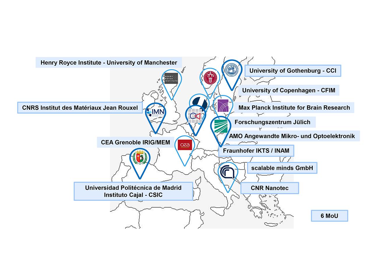
NanoWorldMaps has started the concept phase in 2023. Concepts for the establishment of the nodes and their instrumentation are being developed. Furthermore, processes for access are being defined in order to provide researchers from academia and industry with tailored services.
NanoWorldMaps will become a distributed research infrastructure with internationally distributed imaging nodes, each equipped with a common sub-set of sample preparation and microscopy techniques, including a multi-beam scanning electron microscope, but also complementary microscopy instrumentation e.g. Raman or SIMS for chemical information, or fluorescence microscopy for protein mapping. Additional domain-specific techniques are also likely. Each node would include specialist staff. Users of the imaging service would be supported by specialists in image processing.
NanoWorldMaps members have signed a Memorandum of Understanding (MoU) to support the concept and implementation phase and build a preliminary governance structure. Scientists from academia and industry will benefit from NanoWorldMaps by using open access to cutting-edge 2D/3D imaging technologies combined with pre-defined processes for sample preparation, image acquisition, and data analysis. Microscopy core facilities and centers can profit by becoming one of the distributed NanoWorldMaps nodes.
NanoWorldMaps will enable Ultra-Fast and Extra-Large Area 2D/3D Imaging for material and life scientists
About NanoWorldMaps
NanoWorldMaps works on empowering Europe to lead the revolution in high-throughput multimodal imaging at the nanometer scale. NanoWorldMaps will become a distributed European Research Infrastructure to provide cutting-edge enabling technologies such as Multi-Beam Scanning Electron Microscopy as a service. NanoWorldMaps services will be focused on the needs of scientists from academia and industry in a growing list of strategic application areas.
Literature and image sources
- Zeiss Microscopy GmbH, Oberkochen, Germany
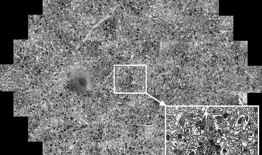
- A connectomic study of a petascale fragment of human cerebral cortex. Preprint available at bioRxiv: https://doi.org/10.1101/2021.05.29.446289