NanoWorldMaps holds Annual Meetings every year. Until today, three meetings were held starting with the 1st Annual Meeting in 2019 at Zeiss Microscopy in Oberkochen, German.
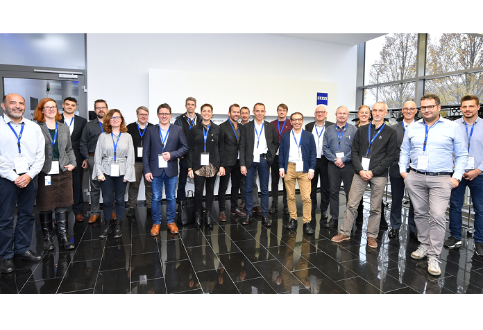
A number of European imaging scientists met on the premises of Carl Zeiss Microscopy in Oberkochen (Germany) to discuss the possible applications of a novel technology that speeds up the acquisition of images from scanning electron microscopy by a factor of one hundred – opening the way to high-resolution 3D imaging. Although initially developed to support the semiconductor industry, this technology has been rapidly adopted particularly by scientists studying brain function through the connections of neurons – so-called connectomics.
All present agreed that the new technology (implemented by Carl Zeiss in their multiSEM instruments) has huge potential, especially when combined with other microscopy techniques for complementary information about the sample. It was decided to attempt to build a new research infrastructure, devoted to large area and large volume imaging at nanometre resolution – NanoWorld Maps.
NanoWorldMaps will enable Ultra-Fast and Extra-Large Area 2D/3D Imaging for material and life scientists
About NanoWorldMaps
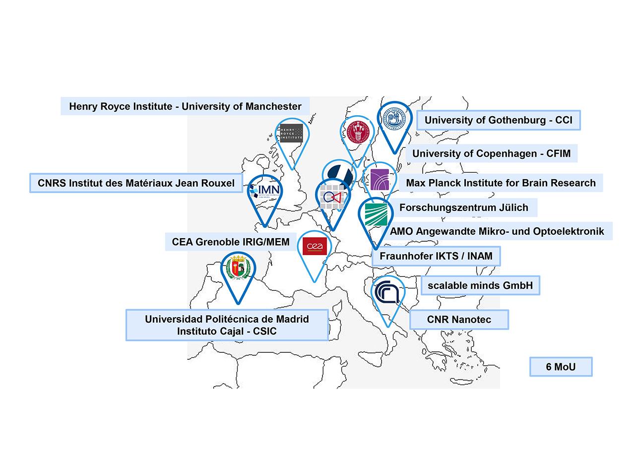
NanoWorldMaps works on empowering Europe to lead the revolution in high-throughput multimodal imaging at the nanometer scale. NanoWorldMaps will become a distributed European Research Infrastructure to provide cutting-edge enabling technologies such as Multi-Beam Scanning Electron Microscopy as a service. NanoWorldMaps services will be focused on the needs of scientists from academia and industry in a growing list of strategic application areas.
Literature and image sources
- Zeiss Microscopy GmbH, Oberkochen, Germany
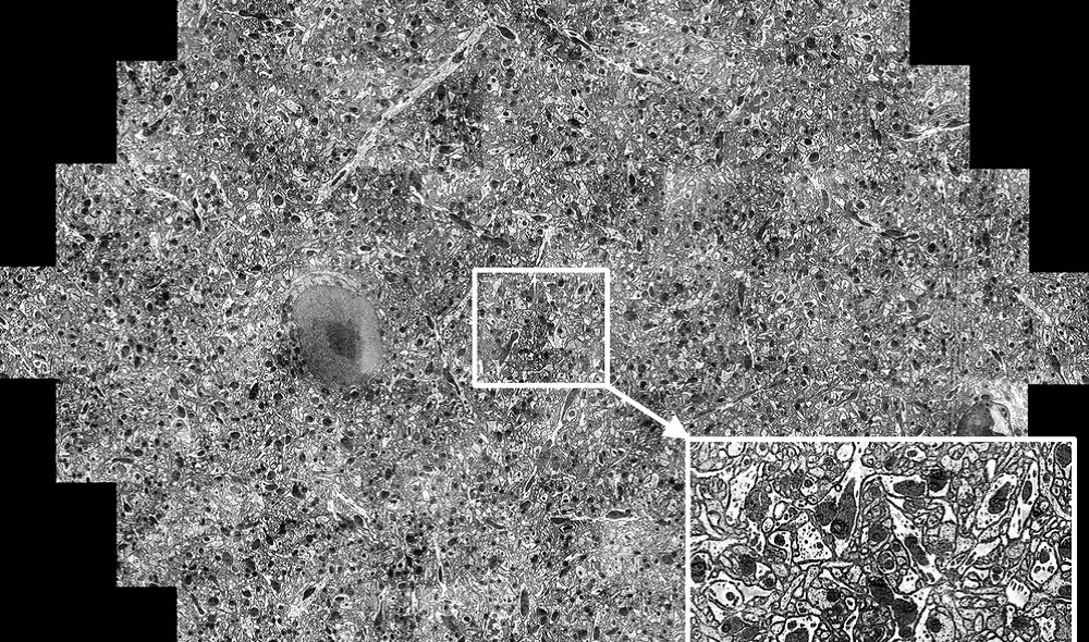
- A connectomic study of a petascale fragment of human cerebral cortex. Preprint available at bioRxiv: https://doi.org/10.1101/2021.05.29.446289